How a PN Junction Diode Works:

The development of the PN Diode is a milestone in the semi-conductor industry because it is a device that essentially is able to control the flow of electricty through a material. More specifically this PN Diode or PN Junction can allow the current
to flow the opposite way in a material.
The first silicon PN Junction was discovered by accident in 1940 ( further reading on this is suggested here to put this discovery in its historical significance).
We now briefly discuss how the PN junction works:
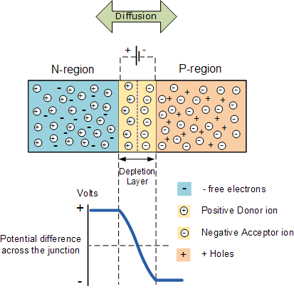
- N refers to Negative charge; this would be material with an excess of free electrons
- P refers to Positive charge;this is material with an excess of what are called "holes". Holes represent places where free electrons used to exist but now have been moved elsewhere. The absence of free negative charge means that there is now positive charge in that area because of the positively charged nuclei.
- Movement across the junction through the depletion layer (see figure above) is done by charge diffusion
This is not complicated to understand. If I have a neutral atom and remove one electron then the atom is positively charged. If the removed electron remains in the vicintiy of the positively charged nucleus then the net charge in that area is zero. However, once the electron becomes free it moves away (via the current in that material) so until new electrons show up in that vicinty, that vicinity is now positively charged. The evacuated electron is the "hole".
To illustrate this process, let's
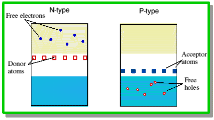
start with two separate pieces of semi conductor material; N-type
and P-type
Now bring them together into one piece to create a "natural" junction.

Free electrons on the n-side meander (through there drift velocity) across the junction and
"drop" into a hole and so charge has vanished.
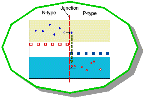
Because of this movement, free electrons near the junction are
depleted leading to a depletion zone located near the actual physical junction (the joining place of N material and P material).

So now if free electrons move into the depletion zone, they feel
the positively charged donor atoms (red squares) and the negatively
charged acceptor atoms (blue squares). These exert a force on the
free charge which keeps it on the N-type side of the junction.
This all works because the donor and acceptor atoms are nuclei that
are fixed in the solid and so the depletion zone is naturally maintained.
To cross the depletion zone, the free electron (charge) requires
extra energy. The junction therefore acts like a barrier, blocking
any charge flow (current) across it.
Supplying a suitable voltage (this applied voltage is sometimes called a bias, or an external bias) will then drive the charge across the
junction. This is why diodes can be made to conduct in only one direction, which
is a very useful property to have.
The PN junction/depletion zone in silicon has a natural electrical field with a potential difference of about 0.6 Volts.
Note: without a voltage being applied, electrons still hop into the conduction band due to temperature fluctuations. This creates the diffusion current. When an electron leaves the valence band and becomes free (i.e. it is in the conduction band) a hole (positive charge) is left. This creates what is known as the drift current and the drift current is very temperature dependent. But even though electrons can cross the junction this is balanced by the subsequent produced holes so no net current actually crosses the junction if the silicon is just sitting there at room temperature. To produce a net current requires application of a voltage
Please take this helpful PN junction self quiz
|