CRT
 LCD Plasma DLP OLED FED
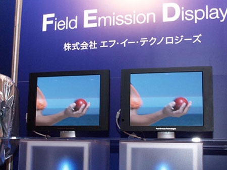
A Carbon NanoTube
Monitor
LCD Plasma DLP OLED FED
A Carbon NanoTube
Monitor
But let's start from the very beginning:
The Cathode Ray Tube: A vacuum glass tube (e.g. the air is removed). An electron beam is emitted and then received on some metal surface. The received energy is converted to a"glow" as a result of interacting with phosphor.
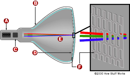
A phosphor is any material that, when exposed to radiation, emits visible light. The incoming radiation can be in the form of an electron beam or in the form of ultraviolet (UV) light.
In a CRT, phosphor coats the inside of the screen. When the electron beam strikes the phosphor, it makes the screen glow. In a black-and-white screen, there is one phosphor that glows white when struck. In a color screen, there are three phosphors arranged as dots or stripes that emit red, green and blue light. There are also three electron beams to illuminate the three different colors together.
However, a television requires an addition element because a television, as is most any image, is a rasterized imaged composed of an array of individual pixels.
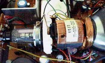
What is therefore required to transform a CRT into a rasterized image, is a mechanism to point and steer the electron beam. Thus a TV CRT is wrapped with steering coils.
The steering coils are simply copper winding that create magnetic fields inside the tube, and the electron beam responds to the fields. One set of coils creates a magnetic field that moves the electron beam vertically, while another set moves the beam horizontally. By controlling the voltages in the coils, you can position the electron beam at any point on the screen.
So the image is created by rapidly moving an electron beam across a raster thus illuminating the phosphor dots. One advantage of the CRT is that each phosphor dot has relatively high brightness.
There are some significant limitations to CRT technology which is why
it never really changed throughout its lifetime (roughly 1950- 2000).
To therefore get to more pixels, HDTV, larger display images, etc one
requires new technologies:
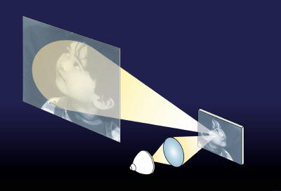
Here a projector (just like the one in class projecting this image), is mounted inside the TV console and projects to a mirror which then reflects the beam to the larger screen. This is a way to make the image size on the CRT screen bigger and the resolution is determined by the number of pixels in the (LCD) projector.
This was first done and made commercially available in 1988 and this really fundamentally changed display technology and allowed for relatively flat screens (hence its possible to make a laptop) of a wide variety of sizes and resolutions.
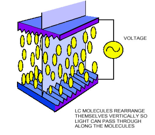
A liquid crystal represents an odd state of matter but one that can be manufactured easily into some materials.
In a solid the molecules always maintain their orientation with respect to each other but in a liquid, the molecules can easily change their oreintation and position with respect to each other.
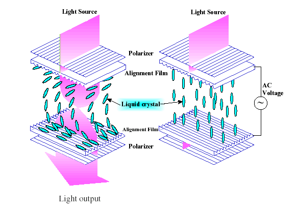
A liquid crystal represents a material where the molecules due maintain their orientation with respect to each other but they can move to different positions. This movement can be controlled by applyin a voltage to the material. In this way, an LCD device is like acts like a "light valve" as its light emitting/transmitting properties can be controlled.
In general, the amount of light intensity per pixel depends upon the applied voltage to that pixel.
In essence, electrical currents can cause liquid crystals to change their shape. This allows them to act as light valves -- different amounts of current allow different amounts of light to pass through the crystal. This lets the LCD device create a greyscale image of different intensities at different locations on the screen.
To add color, most projectors use a series of mirrors that split the light into red, green and blue beams. Each beam passes through a separate LCD, and a lens collects the three beams and projects the image on the screen.
Significant R&D has gone in to the characterization of different materials that can act as an LCD. As shown above, the basic physical size of the LCD is determined by the size and number of molecules that make it up.
But we are not at single molecule devices (yet). Current LCD pixel size is then limited by the electronic interface needed to control the pixel. Improvements (using thin film transistors) have allows for this electronic control interface to become pretty small:
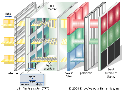
This is why its possible to get 1,000,000 pixels (e.g. 1024x 768) on to a standard laptop screen.
LCD also represents a fairly scalable technology and now 6 million pixel screens as large as 65 inches have been developed.
The basic idea of a plasma display is to illuminate tiny colored fluorescent lights to form an image. Each pixel is made up of three fluorescent lights -- a red light, a green light and a blue light. Just like a CRT television, the plasma display varies the intensities of the different lights to produce a full range of colors.
The central element in a fluorescent light is a plasma - which is an ioniozed gas made up of ions and electrons.
If you introduce many free electrons into the gas by establishing an electrical voltage across it, the situation changes very quickly. The free electrons collide with the atoms, knocking loose other electrons and therefore creating postively charged nuclei.
In a plasma with an electrical current running through it, negatively charged particles are rushing toward the positively charged area of the plasma, and positively charged particles are rushing toward the negatively charged area. This causes energetic collisions which excited the gas atoms in the plasma.
As we learned before, an electron in an excited state will de-excite a lower energy level thus releasing a photon (remember, in a laser this process is tuned so that only a narrow bandwidth of photons are emitted).
In order to produce flouresence, one needs an initial source of UV photons and hence one needs to find the right material to do this. Typically xenon and neon atoms are used in plasma screens as these elements, when excited, produce mostly UV photons.
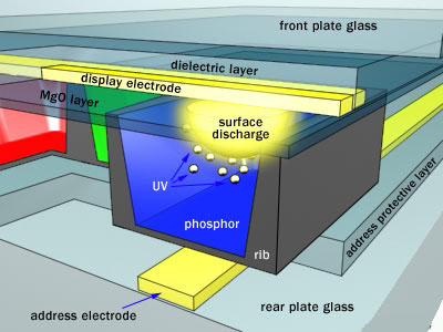
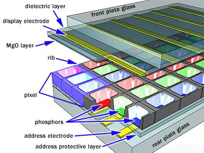
The xenon and neon gas in a plasma television is contained in hundreds of thousands of tiny cells positioned between two plates of glass. Long electrodes are also sandwiched between the glass plates, on both sides of the cells. The address electrodes sit behind the cells, along the rear glass plate. The transparent display electrodes, which are surrounded by an insulating dielectric material and covered by a magnesium oxide protective layer, are mounted above the cell, along the front glass plate.
Both sets of electrodes extend across the entire screen. The display electrodes are arranged in horizontal rows along the screen and the address electrodes are arranged in vertical columns. As you can see in the diagram below, the vertical and horizontal electrodes form a basic grid.
To ionize the gas in a particular cell, the plasma display's computer charges the electrodes that intersect at that cell. It does this thousands of times in a small fraction of a second, charging each cell in turn.
When the intersecting electrodes are charged (with a voltage difference between them), an electric current flows through the gas in the cell. The current creates a rapid flow of charged particles, which stimulates the gas atoms to release ultraviolet photons.
The released ultraviolet photons interact with phosphor material coated on the inside wall of the cell.
The phosphors in a plasma display give off colored light when they are excited. Every pixel is made up of three separate subpixel cells, each with different colored phosphors. One subpixel has a red light phosphor, one subpixel has a green light phosphor and one subpixel has a blue light phosphor. These colors blend together to create the overall color of the pixel. Note that the pixels are layed out horizontally .
By varying the pulses of current flowing through the different cells, the control system can increase or decrease the intensity of each subpixel color to create hundreds of different combinations of red, green and blue. In this way, the control system can produce colors across the entire spectrum.
The main advantage of plasma display technology is that you can produce a very wide screen using extremely thin materials. And because each pixel is lit individually, the image is very bright and looks good from almost every angle.
However, advances in LCD technology have outpaced those in plasma for the most part and its likely that this kind of technology will be phased out over the next few years.
DLP or Digital Light Process works opposite to the principle behind LCDs. LCD displays work by alternately blocking light and letting it through. DLP works by creating images through multiple reflections of light.
These mirrors can switch between ON (where light is fully reflected) and OFF (where light is fully deflected) states. And, by switching between light and dark states at great speeds, these mirrors are able to reproduce the gray scale with staggering accuracy.
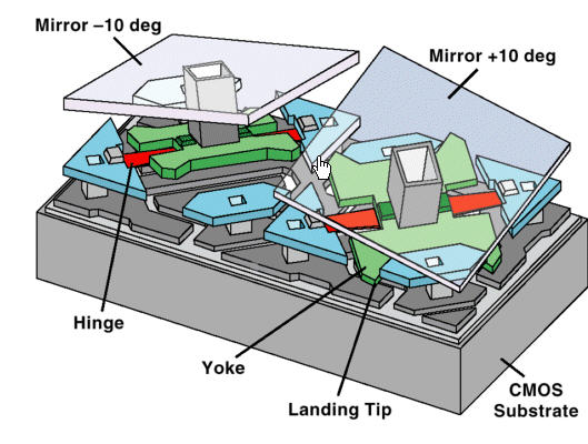
The Digital Micromirror Device (DMD): The functional core of DLP technology is the DMD semiconductor which is operationally defined as a binary spatial light modulator, which just means its a fast ON/OFF swithc.
DMDs contain millions of microscopic mirrors--one for each pixel in their display--that can be directed to tilt 10° back and forth on their axes. These micromirrors are made of aluminum for maximum reflectivity and durability. They measure just 16 x 16 microns or .000256 square mm of reflecting area.
Thus the display is made up literally of millions of tiny mirrors.
The actual number of micromirrors present on a given DMD is equal to the number of pixels on your TV's screen. A display with a resolution of 1280 x 1024 contains a DMD consisting of 1,310,720 micromirrors. This "one pixel, one mirror" setup lends itself to exceptionally precise digital imaging.
The Mirror As Switch: Since each micromirror on a DMD chip operates independent of its neighbors on the DMD grid, each aluminum mirror can reflect light in one of two directions--either 10° toward or 10° away from a lens. The light that gets reflected is directed towards an optical lens, which projects that light onto a screen in the form of a lit pixel.
A light absorber absorbs the light that is deflected away from this lens, so no light reaches the screen at that particular pixel, producing a dark, square pixel image. In short, each micromirror either illuminates a pixel (i.e., switches it ON by moving +10 degrees) or darkens a pixel (i.e., switches it OFF by moving -10 degrees ).
Since your eye can only process image information at rate of about 30 milliseconds, then fast switching between light and dark would produce some value of gray, according to your eye-brain.
Grays are encoded in bit planes that represent the ratio of light states to dark ones. A pixel's relative brightness is written in 8- or 10-bit segments, with each bit representing successively longer on/off durations.
In an 8-bit word, for example, the time durations have relative values of 20, 21, 22, 23, -- 27, which allows for 256 unique combinations of ones and zeroes or lights and darks.
Each pixel is thus capable of displaying 256 levels of gray. A 10-bit image processing would display 1024 levels of gray.
This technique for producing the sensation of the gray scale before a viewer's eyes is called binary pulsewidth modulation.
Tp produce color, DLPs utilize a color wheel composed of red, green, and blue filters, which direct individual pulses of colored light toward the DMD for gray-scale processing. This means that, at any given instant, only one of the primary light colors is hitting the DMD, but when the filter system spins fast enough (~120 times per second), the colors appear blended into a full-color digital image.
DLPs display color images as rapid sequences of red, green, and blue light signals, which the brain effectively integrates into one signal. For 8 bits this is 256 x 256 x256 shades of RGB = 16.8 million different colors.
The principle advantage of DLP is that its basically a bit by bit matching of the output, viewed by the viewer, to the actual digital input.
One facet of all the previous technologies lies in their arrangements of individual R, G, and B pixels (or sub-pixels). In general, this arrangement is such that the pixels are laid out on a horizontal substrate.
To attain the goal of cramming more pixels into the same amount of physical area, requires moving to some vertical arrangement where the individual RGB elements are stacked on top of one another.
![]()
One key to making the vertical pixel rely's on the fact that photons of different energy (e.g. wavelength, color) can penetrate silicon to different levels of depth. Photons with the shortest wavelength have the shortest penetration lengths (due to more interactions with the atoms).
So in principle, one can make this kind of pixel device:
The layers are positioned to take advantage of the fact that silicon absorbs different wavelengths of light to different depths. The bottom layer records red, the middle layer records green, and the top layer records blue. Each stack of pixels directly records all of the light at each point in the image.
Until recently, this scheme was difficult to engineer on a commercial scale due to various processing problems and the need for the thicknesses of the respective silicon layers to be very precise. This limitations are now over come, and if you can afford one, this is by far the the best digital slr camera out there
The latest revolution in display technology involves Organic Light Emitting Diodes (OLEDs).

The tremendous advantage of OLED pixels is that they can be affixed to flexible surfaces (e.g. your clothing). The disadvantage is that organic material decays and therefore the display surface does have to be periodically refreshed.
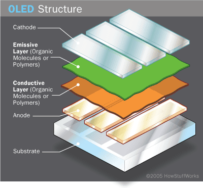
Various designer polymers (polyaniline, plyfluorene) can be used in the organic layers.
OLEDs emit light in a similar manner to regular LEDs, through a process called electrophosphorescence.
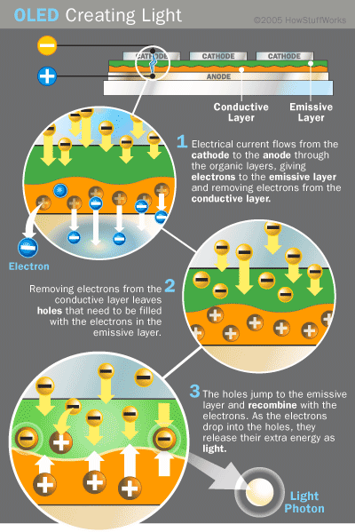
The basic process works like this:
OLED Advantages and Disadvantages:
OLEDs offer many advantages over both LCDs and LEDs:
Problems with OLED:
Field Emission Displays
The FED is a new type of flat-panel display in which electron emitters, arranged in a grid, function individually to generate colored light. It may be a breakthrough technology because it can accommodate a thin panel like liquid crystal display (LCD) and offers a wider field-of-view and higher image quality.
Field-emission displays use much less power than plasma displays because they’re intrinsically more efficient.
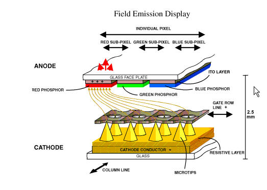
The key feature likes in the "cathode tips" which are carbon nanontubes that serve as the electron gun. In that since, FED works like a CRT with multiple electron guns at each pixel.
Potential advantages of FEDs: