Physics 155 Midterm
Name: _______________________________
Student ID:_________________________
This exam consists of 15 short/medium answer questions. Questions are either worth 10, 15 or 20 points. There are a total of 200 points available on the exam.
Write Legibly and Carefully - Sloppily prepared exams will receive a point deduction. Take your time on this exam, there is no reason to hurry through it.
In all of the questions below, please confine your answers to the space that is provided for that question. For any numerical question, be sure to show your work, don't just write down an answer.
10 Point Questions
- You have just purchased a new digital camera. The specifications tell you that you have 10 Megapixels and that each pixel has a depth of 32 bits. How much storage, in units of Megabytes is required for one image.
(10,000,000 x 32 bits)/8
= 40 megs
- Explain the basic concept of a "switched information network"
Basic idea is that
information is routed via physically different carriers (i.e. the Pony express
model); information is not routed along one single route with one single
carrier.
- Explain the basic concept of the "bit" and what a bit is designed to represent:
A bit is a discrete piece
of information. It represents a physical state (heads/tails; voltage ON;
Voltage OFF; electron present; no electron present). Various protocols can then
be built to assemble bits into different kinds of information.
- Explain the origin of shot noise in an electrical circuit.
Fluctuations
in the number density of carriers (electrons) usually as result of current
injection in some part of the overall circuit. Also occurs for weak signal situations as some electrons are
just lost.
- Provide brief definitions of the concepts of network latency and packet loss.
Network latency = physical
transit time between packets sent and acknowledgement of receipt
Packet loss = drop out of packets in the bit stream which requires a
retransmittal of the whole packet
- Explain why it is necessary to dope silicon in order to improve its conductivity.
Key points:
a) at
room temperature, silicon has a very low density of free charges and thus can't
really carry a current
b) phosphorous has 5 valence
electrons but only 4 are needed for silicon; therefore when you introduce
phosphorous you automatically get a free electron and the free charge density
is increased.
- Explain the basic difference between an AND logic gate and an OR logic gate, in the case where each gate has 2 inputs:
AND: 1 true state; 3 false
states; both inputs have to be high (1) in order to ouput
a high state (1 or ON)
OR: 1 false state; 3 true states; if either or both inputs is high then the gate returns a high state:
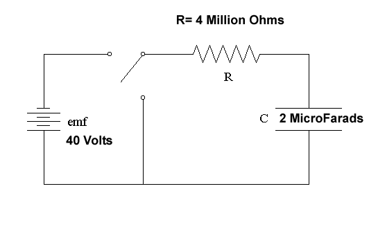
- Examine the RC Circuit that is shown below. What is the time constant of this circuit and how much current will flow through the circuit 8 seconds after the switch is turned off.
RxC = 8 seconds; current = 10 microamps (V/R); after 16 second current has fallen by 10*e-2
15 Point Questions
- Explain what random and systematic errors are as applied to measurements. What techniques can be used to minimize their effects on the integrity of the data?
Random Errors: Increases
variability around the mean but does not change the mean.
Systematic Error: Occurs from a bias in the measurement system or a
calibration error and thus alters the mean value of the measurement
Random errors can be overcome (minimized) by using a more accurate
instrument or by taking lots of data. Systematic error can be overcome by doing
independent calibration checks of the device.
- Explain how the photoelectric effect shows that light can behave like a particle.
Two main points:
1. Ejected electrons occur
as a function of frequency of the light; not its intensity. This implies there
is a threshold energy required for the ejection of electrons since energy of a
photon depends on its frequency. (This crucial point was left out by many
responses)
2. Ejected electrons occur without a time delay; if energy was in a wave,
there would be time needed for the device to absorb that energy.
- Explain the basic operating
principles of a transistor and its overall purpose in an electronic
circuit:
Operating principles: source, gate, drain à voltage applied to
gate allows current to flow from source to drain (this part was left out of
most responses)
Overall purpose: A transistor acts like a “valve”
and controls the rate and flow of information (e.g. electrons) through a
circuit.
- Explain how the "depletion zone" forms in a semi-conductor material and how its presence serves to make a PN junction function as a diode.
Generally well done:
Basic answer:
In a PN junction the N side has electrons and the P side has holes (+
charge). When electrons flow across
the depletion zone they combine with the holes and charge vanishes. To make more electrons cross the
depletion zone requires extra energy. Thus the depletion zone serves as a
barrier to natural electron transport (as it blocks the flow of charge) meaning
that the PN junction now can serve as a diode in which the flow of electricity
can be directed one way.
20 Point Questions
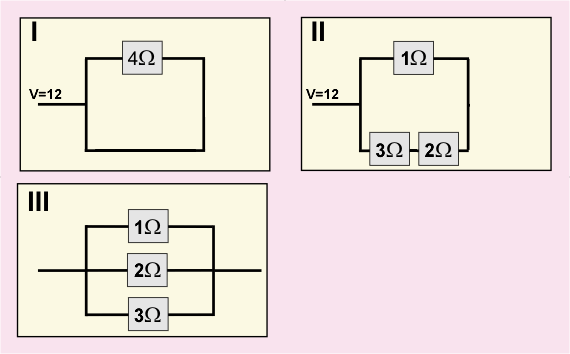
- Examine the Circuits below and show all your work.
- What is the total current in circuit I
V = R * I; I = 12/4 = 3 amps
- What is the total resistance in circuit II and III
II = series = 1 + 2 +3 =
6
III = parallel: 1/R = 1/1 + 1/2 +1/3 = 11/6; R = 6/11 Ohms
- What is the voltage drop across the top resistor
in Circuit II?
V = R * I; V = 12; R =6
so I=2 for the whole circuit
At top resistor V = R*I; R=1; I=2 so V = 2

- What is meant by the valence band and the conduction band in metals and/or semi-conductors? Using those concepts of energy bands, explain what makes one material a conductor and another material a semi-conductor
Conduction band refers to electrons which are free of any atoms and
therefore can flow through the material.
Metals have lots of the conduction band states full because of low
band gap energy between valence and conduction state and the fact that each
atom has a lot of electrons. So it’s easy for many of those electrons to
fill the conduction band energy states to make that material a good conductor.
A semi-conductor has a fairly large band gap energy (compared to a
conductor) so that it’s difficult to give the device enough energy to
cause the electrons to hope from the valence band to the conductor band. The
fact that hops are possible under some conditions (usually via thermal
fluctuations) means the material is a semi-conductor.
In general, the density of free electrons in a semi-conductor is at
least 106 times smaller than a conductor.
- Explain in general terms some of the obstacles that need to be overcome so that the commercial world can move from discovery physics (i.e. the photoelectric effect, the quantum nature of charge, the properties of semi-conductors) to the manufacturing of real devices that apply this physics.
