The Evolution of Display Technologies Continued
Stage 4: DLP: Many moving mirrors
DLP or Digital Light Process works opposite to the principle behind
LCDs. LCD displays work by alternately blocking light and letting it
through. DLP works by creating images through multiple reflections of
light.
These mirrors can switch between ON (where light is fully reflected) and OFF (where light is fully deflected) states. And, by switching between light and dark states at great speeds, these mirrors are able to reproduce the gray scale with staggering accuracy.
The Digital Micromirror Device (DMD): The functional core of DLP technology is the DMD semiconductor which is operationally defined as a binary spatial light modulator, which just means its a fast ON/OFF swithc.
DMDs contain millions of microscopic mirrors--one for each pixel in their display--that can be directed to tilt 10 back and forth on their axes. These micromirrors are made of aluminum for maximum reflectivity and durability. They measure just 16 x 16 microns or .000256 square mm of reflecting area.
Thus the display is made up literally of millions of tiny mirrors. The actual number of micromirrors present on a given DMD is equal to the number of pixels on your TV's screen. A display with a resolution of 1280 x 1024 contains a DMD consisting of 1,310,720 micromirrors. This "one pixel, one mirror" setup lends itself to exceptionally precise digital imaging.
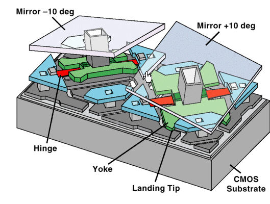
The Mirror As Switch: Since each micromirror on a DMD chip operates independent of its neighbors on the DMD grid, each aluminum mirror can reflect light in one of two directions--either 10 toward or 10 away from a lens. The light that gets reflected is directed towards an optical lens, which projects that light onto a screen in the form of a lit pixel.
A light absorber absorbs the light that is deflected away from this lens, so no light reaches the screen at that particular pixel, producing a dark, square pixel image. In short, each micromirror either illuminates a pixel (i.e., switches it ON by moving +10 degrees) or darkens a pixel (i.e., switches it OFF by moving -10 degrees ).
Since your eye can only process image information at rate of about 30
milliseconds, then fast switching between light and dark would produce
some value of gray, according to your eye-brain.
Grays are encoded in bit planes that represent the ratio of light states to dark ones. A pixel's relative brightness is written in 8- or 10-bit segments, with each bit representing successively longer on/off durations. In an 8-bit word, for example, the time durations have relative values of 20, 21, 22, 23, -- 27, which allows for 256 unique combinations of ones and zeroes or lights and darks. Each pixel is thus capable of displaying 256 levels of gray. A 10-bit image processing would
display 1024 levels of gray.
This technique for producing the sensation of the gray scale before a viewer's eyes is called binary pulsewidth modulation.
To produce color, DLPs utilize a color wheel composed of red, green, and blue filters, which direct individual pulses of colored light toward the DMD for gray-scale processing. This means that, at any given instant, only one of the primary light colors is hitting the DMD, but when the filter system spins fast enough (~120 times per second), the colors appear blended into a full-color digital image.
DLPs display color images as rapid sequences of red, green, and blue light signals, which the brain effectively integrates into one signal. For 8 bits this is 256 x 256 x 256
shades of RGB = 16.8 million different colors.
The principle advantage of DLP is that its basically a bit by bit matching
of the output, viewed by the viewer, to the actual digital input.
Stage 5: The development of vertical or stacked pixels
One facet of all the previous technologies lies in their horizontal arrangement
of individual R, G, and B pixels (or sub-pixels).
To attain the goal of cramming more pixels into the same amount of
physical area, requires moving to some vertical arrangement where the
individual RGB elements are stacked on top of one another.
One key to making the vertical pixel rely's on the fact that photons
of different energy (e.g. wavelength, color) can penetrate silicon to
different levels of depth. Photons with the shortest wavelength have
the shortest penetration lengths (due to more interactions with the
atoms).
So in principle, one can make this kind of pixel device:
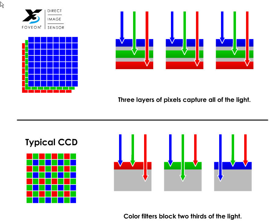
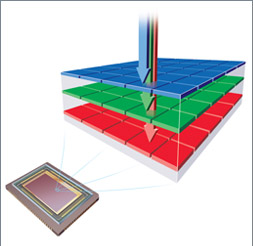
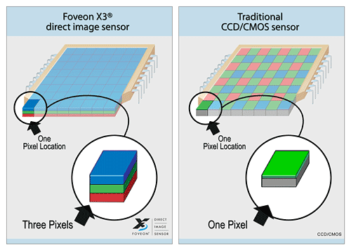
The layers are positioned to take advantage of the fact that silicon absorbs
different wavelengths of light to different depths. The bottom layer records red,
the middle layer records green, and the top layer records blue. Each stack of pixels
directly records all of the light at each point in the image.
Until recently, this scheme was difficult to engineer on a commercial scale
due to various processing problems and the need for the thicknesses of the
respective silicon layers to be very precise. This limitations are now
over come, and if you can afford one, this is by far the the best digital slr camera out there
Stage 6: Using Organic Stacked pixels
The latest revolution in display technology involves Organic Light Emitting
Diodes (OLEDs).
Samsung 40 Inch OLED Monitor

The tremendous advantage of OLED pixels is that they can be affixed to
flexible surfaces (e.g. your clothing). The disadvantage is that organic
material decays and therefore the display surface does have to be
periodically refreshed.
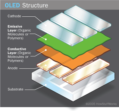 An OLED consists of the following parts:
- Substrate (clear plastic, glass, foil) - The substrate supports the OLED.
- Anode (transparent) - The anode removes electrons (adds electron "holes") when a current flows through the device.
- Organic layers - These layers are made of organic molecules or polymers.
- Conducting layer - This layer is made of organic plastic molecules that transport "holes" from the anode.
- Emissive layer - This layer is made of organic plastic molecules (different ones from the conducting layer) that transport electrons from the cathode; this is where light is made.
- Cathode (may or may not be transparent depending on the type of OLED) - The cathode injects electrons when a current flows through the
device.
Various designer polymers (polyaniline, plyfluorene) can be used in
the organic layers.
OLEDs emit light in a similar manner to regular LEDs, through a process called electrophosphorescence.
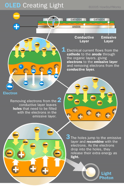
The basic process works like this:
- A voltage is applied across the OLED
- Electrical current flows from the cathode to the anode through
the organic layers. The cathode injects electrons to the
emissive layer; the anode injects holes into the conductive layer
- At the boundary between the emissive and conductive layers, the
electrons recombine with the holes and transition down atomic energy
levels.
- The OLED emits light
- The color of the emitted light depends on the type of organic
molecule in the emissive layer. Different molecules within the layer
can give different colors and hence a vertically stacked arrangement
of RGB can occur.
- The intensity of the light is proportional to the amount of supplied
current, so, like an LCD, intensity per pixel can be controlled.
OLEDs offer many advantages over both LCDs and LEDs:
- The plastic, organic layers of an OLED are thinner, lighter and more flexible than the crystalline layers in an LED or LCD.
Because the light-emitting layers of an OLED are lighter, the substrate of an OLED can be flexible instead of rigid. OLED substrates can be plastic rather than the glass used for LEDs and LCDs.
- OLEDs are brighter than LEDs. Because the organic layers of an OLED are much thinner than the corresponding inorganic crystal layers of an LED, the conductive and emissive layers of an OLED can be multi-layered. Also, LEDs and LCDs require glass for support, and glass absorbs some light. OLEDs do not require glass.
-
Because OLEDs do not require backlighting, they consume much less power than LCDs (most of the LCD power goes to the backlighting). This is especially important for battery-operated devices such as cell phones.
-
OLEDs are easier to produce and can be made to larger sizes. Because OLEDs are essentially plastics, they can be made into large, thin sheets. It is much more difficult to grow and lay down so many liquid crystals.
Problems with OLED:
- Lifetime - While red and green OLED films have longer lifetimes (46,000 to 230,000 hours), blue organics currently have much shorter lifetimes (up to around 14,000 hours). That's less than 2 years of continuous use.
- Manufacturing - Manufacturing processes are expensive right now so
these devices are not yet near consumer price points.
Stage 7:
Carbon Nanotube pixels
Field Emission Displays
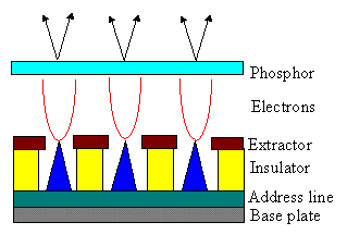
The FED is a new type of flat-panel display in which electron emitters, arranged in a grid, function individually to generate colored light. It may be a breakthrough technology because it can accommodate a thin panel like liquid crystal display (LCD) and offers a wider field-of-view and higher image quality.
Field-emission displays use much less power than plasma displays because they re intrinsically more efficient.
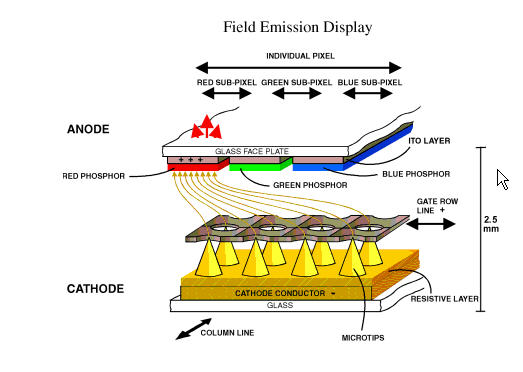
The key feature likes in the "cathode tips" which are carbon nanontubes
that serve as the electron gun. In that since, FED works like a CRT with
multiple electron guns at each pixel.
Potential advantages of FEDs:
- The electron gun can be very well localized and the subsequent
pixels can be made quite small. Therefore resolution elements can be
increased per physical area. This has important applications to mobile
devices which are likely the main market driver.
- Power consumption is dependent on the actual display content.
- Pixel response time (refresh rate) is much faster than TFT LCD
response times.
- Individual pixel brightnesses can be quite high.
Currently tho, there is no production scale involved in the creation
of the necessary carbon nanotubes (CNT). Samsung appears to have
proprietry leader in the production of CNTs and you may want to invest
with them.
|