Basics of SemiConductors:
 All consumer electronics rely on the use
of semiconductors to function. All consumer electronics rely on the use
of semiconductors to function.
The physics that governs the movement of electrons (which are extremely
tiny objects) is based on quantum mechanics and not classical Newtonian
physics.
This is not a course about quantum mechanics so don't suddenly freak
out.
Rather, we will use some important principles quantum mechanics to better
understand how semiconductors work.
To begin with, we will consider a solid (like a semi-conductor) as
any material in which the atoms are arranged in an ordered fashion.
Such ordered is usually referred to as a crystal or a lattice.
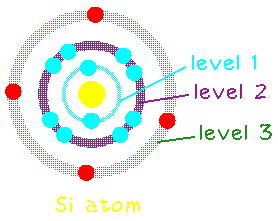
Let's consider the case of silicon.
Silicon has 14 electrons, but only the outer most 4 are available as
"valence" electrons to help bond with other atoms.
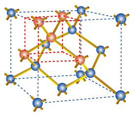
In its solid form, each silicon atom normally shares one of its four valence electrons in a covalent bond with each of four neighboring silicon atoms. The solid thus consists of basic units of five silicon atoms: the original atom plus the four other atoms with which it shares valence electrons.
In two dimensions we can represent silicon as below
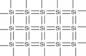
Each silicon atom shares its four valence electrons with valence electrons from four nearest neighbors, filling the shell to 8 electrons, and forming a stable, periodic structure.
Once the atoms have been arranged like this, the outer valence electrons are no longer strongly bound to the host atom. Therefore, in principle, these
outer electrons can easily be "freed" from the lattice and move through
the material. The movement of electrons through material is a current.
The outer shells of all of the atoms blend together and form what is called a band. This band is called the conduction band .
Electrons that are still bound in atoms are said to be in the valence band .
The difference in energy between these two bands is called
the bandgap energy
However,
due to those pesky quantum mechanical effects, there is not just one band which holds electrons, but several of them.
What matters in the physics is both the spatial distribution of the
electrons in the solid as well as their distribution in
energy. This energy distribution is periodic in nature and is driven
by the existence of positively charged atomic nuclei which are arranged
in a crystal in a regular array. Thus, as electrons move through the crystal
they will be exposed to periodic proximities to these positive nuclei.
The interaction between electrons and nuclei is complicated and involves
something called the electronic wave function.
This is well beyond the scope of this course but it had to be worked
out in detail before semiconductors could be well understood physically.
The essential point is, due to quantum mechanics, electrons are not
allowed to have any arbitrary value of energy in a solid. That is,
there are only a certain number of allowable
states for the electrons to fill.
Consider the diagram below which shows two bands of some substance, where
the second band is of higher energy than the first band. The energy
difference between the two bands is the Band Gap.
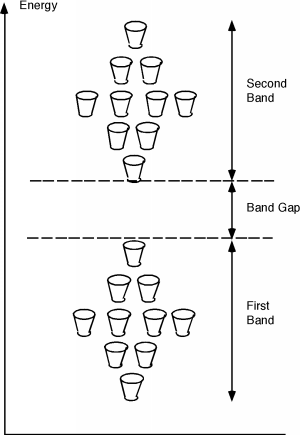 The cups in the figure represent the allowed states
that electrons can occupy in a periodic solid. Note, that these
allowed states are grouped within relatively small energy ranges.
As you move up in energy you encounter the first energy band, with
very few allowed states (e.g. 1 cup). The "center" of that energy band
has the most allowable states (e.g. 4 cups) and as you move away from
that center band energy, the number of allowable states decreases.
Then you enter the band gap region which has no cups (e.g. no allowable
states). The you enter another band, with an energy distribution of
allowable states (e.g. the cup configuration) that is similar to the
previous band.
Most materials have several of these bands, not just 2.
The cups in the figure represent the allowed states
that electrons can occupy in a periodic solid. Note, that these
allowed states are grouped within relatively small energy ranges.
As you move up in energy you encounter the first energy band, with
very few allowed states (e.g. 1 cup). The "center" of that energy band
has the most allowable states (e.g. 4 cups) and as you move away from
that center band energy, the number of allowable states decreases.
Then you enter the band gap region which has no cups (e.g. no allowable
states). The you enter another band, with an energy distribution of
allowable states (e.g. the cup configuration) that is similar to the
previous band.
Most materials have several of these bands, not just 2.
Now there is a rule: each band has exactly 2N allowed states in it,
where N is the total number of atoms in the particular crystal. For
our schematic case, N=5 so that 2N = 10, so that there are 10 cups
in each band.
Into each band we must now distribute all of the valence electrons
associated with the atoms.
However, there is a very important restriction
only one electron can occupy each allowed state
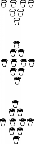 So if the first cup in the first band is filled, then an electron
necessarily must move to a higher energy to fill another state (cup).
For silicon, which has 4 valence electrons per atom, then, since
we have 5 atoms, we would simply fill all 20 cups with valence electrons
in the first two states.
In this case we have run out of electrons to fill the cups in the third
band. To get the cups in the third band filled, the electrons in
silicon would have to acquire a relatively large amount of energy
Hence if you applied a voltage to silicon (e.g. an electric field),
that voltage would have to be higher than the band gap energy between
the second and third bands - thus electrons in silicon can not easily
gain energy and this makes it a poor conductor of electricity under normal circumstances. So how can we cause silicon to be
a conductor at all?
Well, the schematic case demonstrated of the first 20 cups being
full for silicon really only occurs at zero temperature.
At room temperature, the electrons gain some thermal energy and
move to the higher energy band.
So if the first cup in the first band is filled, then an electron
necessarily must move to a higher energy to fill another state (cup).
For silicon, which has 4 valence electrons per atom, then, since
we have 5 atoms, we would simply fill all 20 cups with valence electrons
in the first two states.
In this case we have run out of electrons to fill the cups in the third
band. To get the cups in the third band filled, the electrons in
silicon would have to acquire a relatively large amount of energy
Hence if you applied a voltage to silicon (e.g. an electric field),
that voltage would have to be higher than the band gap energy between
the second and third bands - thus electrons in silicon can not easily
gain energy and this makes it a poor conductor of electricity under normal circumstances. So how can we cause silicon to be
a conductor at all?
Well, the schematic case demonstrated of the first 20 cups being
full for silicon really only occurs at zero temperature.
At room temperature, the electrons gain some thermal energy and
move to the higher energy band. 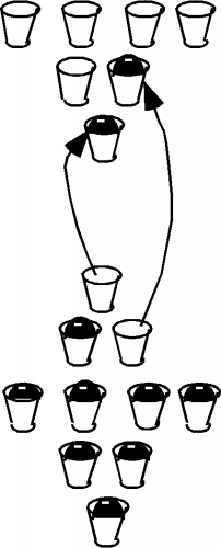 This is called "hopping the gap"
and is shown schematically to the left.
Well if this process were efficient, then we can turn silicon into a good
conductor of electricity just by heating it up. But, life is not
that simple and to really make silicon conduct electricity will require
the introduction of other atoms (in a process called doping) into
silicon. We will get to doping shortly, but for now, back to pure
silicon.
This is called "hopping the gap"
and is shown schematically to the left.
Well if this process were efficient, then we can turn silicon into a good
conductor of electricity just by heating it up. But, life is not
that simple and to really make silicon conduct electricity will require
the introduction of other atoms (in a process called doping) into
silicon. We will get to doping shortly, but for now, back to pure
silicon.
In silicon at room temperature, about 10 billion electrons per cc are
thermally excited from the valence band to the conduction band. As you heat up the silicon, for instance, exposing it to sunlight, more and more valence band electrons can hop to the conducting band causing current flow. This is basically how a solar photovoltaic cell works. In the world of electrons, we replace solar energy with an applied voltage to the silicon which serves as an energy input thus facilitationg the hopping of electrons and the formation of a current flow thorugh the silicon which now makes it a conductor of electricity.
|