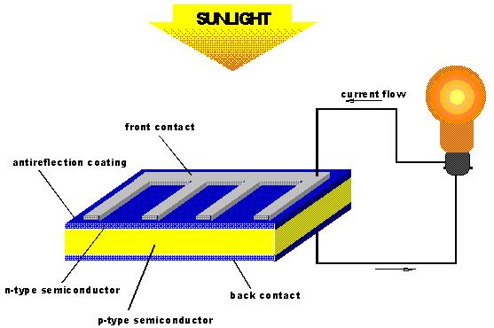
 Photovoltaics; conversion of solar photons into electrons that
flow down a semi-conductor.
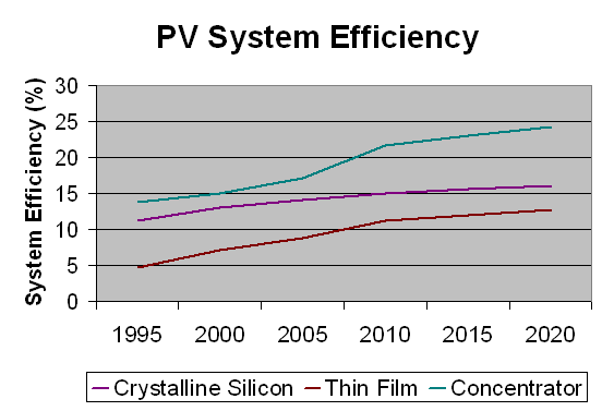
Main problem is low efficiency (about 10%).
Photovoltaics; conversion of solar photons into electrons that
flow down a semi-conductor.
Main problem is low efficiency (about 10%).
Direct conversion into electricity
Photovoltaics; conversion of solar photons into electrons that
flow down a semi-conductor.
Main problem is low efficiency (about 10%).
Charge Generation
 Photoelectric Effect
To make use of the photoelectric effect, we need material that is a good conductor of electricity and which can be manufactured in bulk at reasonable cost. This conditions strongly constrain the available choices. For most practical aspects, Silicon is the material of choice.
Silicon:
To begin with, we will consider a solid (like a semi-conductor) as
any material in which the atoms are arranged in an ordered fashion.
Such ordered is usually referred to as a crystal or a lattice.
Let's consider the case of silicon.
Silicon has 14 electrons, but only the outer most 4 are available as
"valence" electrons to help bond with other atoms.
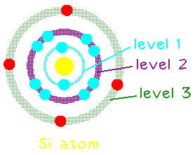
In two dimensions we can represent silicon as below
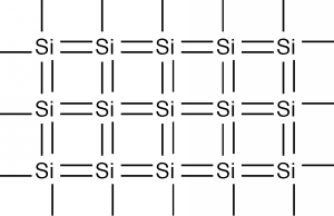
Each silicon atom shares its four valence electrons with valence electrons from four nearest neighbors, filling the shell to 8 electrons, and forming a stable, periodic structure.
Once the atoms have been arranged like this, the outer valence electrons are no longer strongly bound to the host atom. Therefore, in principle, thse outer electrons can easily be "freed" from the lattice and move through the material. The movement of electrons through material is a current.
The outer shells of all of the atoms blend together and form what is called a band. This band is called the conduction band . Electrons that are still bound in atoms are said to be in the valence band .
The difference in energy between these two bands is called the bandgap energy
For a solar energy application, we must find a material in which there is a good match between the band gap and the incoming energy spectrum of solar radiation.
Fortunately, silicon suffices and its very abundant and easily mined from the earth's crust.
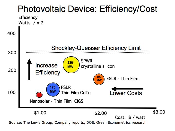
Note: more exotic materials can be used to make a solar cell and make a more efficient one but none of those materials has any cost-effective mass production ability.
Schematic structure of energy bands in Silicon:

So much energy is 1.11 Electron Volts?

You can not defeat this fundamental piece
of physics without paying an even larger energy cost in cooling.
Note that all measures of PV efficiency are made a 0 degrees C when done in a lab. "Rated" efficiencies are usually done at a standard temperature of 25 C.
In general:
Important Notes:
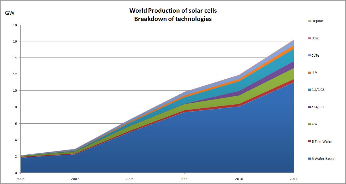
We are limited in copper and sellenium
Cadmium is toxic and banned in many countries; The abundance of Tellerium is
15-30 times less than the abundance of Platinum
What's unique about this class: We interrogate the real world!
Notes:
Recently, a new dimension to this problem is being researched and developed
Organic Solar Cells: (a.k.a. Light Harvesting devices)
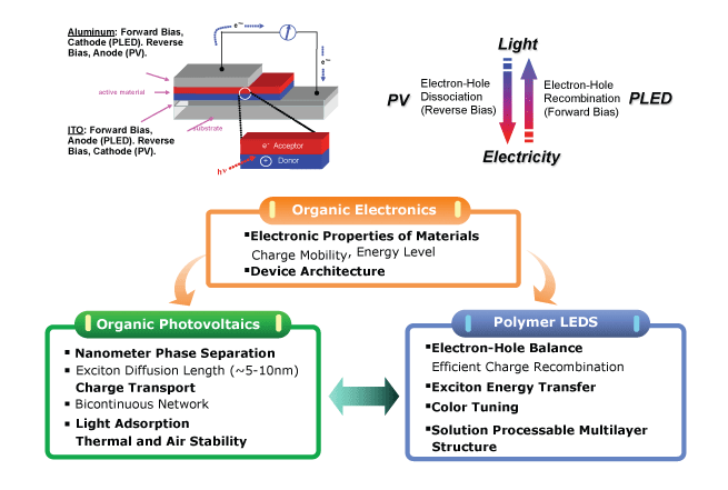
In essence, the electronic properties of semiconductors (e.g. silicon) can now be mimicked by the use of organic materials, dyes, etc, as means or separating out electrons from the material.
Advantages:
Disadvantages: